


Description
Product Overview
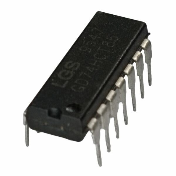
CD4094B Shift Register
The CD4094B consists of an 8-bit shift register and a 3- STATE 8-bit latch. Data is shifted serially through the shift register on the positive transition of the clock. The output of the last stage (QS) can be used to cascade several devices. The QS output transfers data to a second output, Q¢S, on the following negative clock edge
The output of each stage of the shift register feeds a latch,which latches data on the negative edge of the STROBE input. When STROBE is HIGH, data propagates through the latch to 3-STATE output gates. When you take OUTPUT ENABLE HIGH, these gates enable.
Features of CD4094B Shift Register
- Wide supply voltage range: 3.0V to 18V
- High noise immunity: 0.45 VDD (typ.)
- Low power TTL compatibility: Fan out of 2 driving 74L or 1 driving 74LS
- 3-STATE outputs
Recommended Operating Conditions
- DC Supply Voltage (VDD) : +3.0 to +15 VDC
- Input Voltage (VIN) : 0 to VDD VDC
- Operating Temperature Range (TA) : -40°C to +85°C


Reviews
There are no reviews yet.